News
Momentum Builds for Manufacturer of Breakthrough 'repeatable Carbon Nanotube Growth' Tool
Nov 29 2007
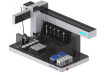
Surrey NanoSystems is currently building its third NanoGrowth system for fabricating carbon nanotube structures, and is rapidly commercialising its technology. Two aspects of the company's unique intellectual property are driving market interest: the very high degree of precision and repeatability built into the tool, and the ability to grow materials at low temperatures that are compatible with commercial semiconductor processes. At the MRS Fall Exhibit, Surrey NanoSystems' Chief Scientist Dr Guan Yow Chen will be on hand to discuss and advise on tool configurations for commercial applications and research projects.
"At this early stage in the cycle for applying new carbon nanotube materials commercially, the requirement for a stable platform capable of prototyping and fabricating structures repeatably is critical. Our unique tool design provides this capability, combined with flexibility that allows configurations to be built to serve individual development ideas. The tool's intrinsic modularity allows users to gain automated control over all aspect of nanomaterial synthesis, from catalyst generation to final material processing," says Dr Guan Yow Chen of Surrey NanoSystems.
He continues: "I'm able to discuss the processing techniques and results that the company has gained from our development partnership with the University of Surrey's Advanced Technology Institute, plus a parallel agreement that we now have in place with a major European research laboratory, who are helping us with independent test-bed services for our unique processing recipes."
The company's first tool is NanoGrowth 1000n, which comes with both CVD (chemical vapor deposition) and PECVD (plasma-enhanced CVD) processing capability. These two techniques provide great processing versatility for users. Precision fabrication and configuration repeatability principles are at the core of the tool's architecture, which has been developed by engineers with many years of experience of creating thin-film tools for both scientific research and commercial fabrication. Among many quality-oriented architectural features are an ultra-high purity gas delivery system and flexible closed-loop control systems that allow users to define target tolerances to achieve a high level of repeatability during all phases of the process. Field-proven carbon nanotube fabrication programs are provided with the tool in the form of software templates that may be adapted easily by users for their own applications.
A high degree of hardware modularity further extends the capability of the tool's design, as it facilitates easy expansion and configuration to meet current and future fabrication requirements. Among many options are further processing techniques such as ICP (inductively coupled plasma), dual sputter sources for catalyst deposition - including a module for delivery of vapor-phase catalysts like ferrocene - and modules to add process stages for automated pilot production or high throughput. Included in the latter category are an automated wafer transport load/lock system, integrated etching capability, and a PECVD module for deposition of thin-film silicon-based materials.
Digital Edition
Lab Asia Dec 2025
December 2025
Chromatography Articles- Cutting-edge sample preparation tools help laboratories to stay ahead of the curveMass Spectrometry & Spectroscopy Articles- Unlocking the complexity of metabolomics: Pushi...
View all digital editions


Events
Jan 21 2026 Tokyo, Japan
Jan 28 2026 Tokyo, Japan
Jan 29 2026 New Delhi, India
Feb 07 2026 Boston, MA, USA
Asia Pharma Expo/Asia Lab Expo
Feb 12 2026 Dhaka, Bangladesh